Pinhole Camera Project

After coming back to the Lab after some time away, I’ve found that I need to work on my own to produce a project; I had already considered ideas in the weeks prior to this so I had a good idea of what I wanted to achieve. I figured that I could create my own pinhole camera by using a button, an arduino board and a servo motor. My concept would be made in such a way that the servo would be attached to a piece of material that would cover the pinhole and, when activated, the servo would move the material and would allow light to pass through to expose the inside of the box to light.

In order to make this a reality, I need to code an arduino board to tell a servo motor to move 90 degress when a button is pressed, wait 30 seconds and then move back to its original state. This would allow for a 30 second exposure in the camera.

I have been using tinkercad to attempt to achieve this. After trying different attempts using the ‘block’ method of coding that is used in tinkercad, I could not get the servo to do what I wanted. In an attempt to fix this, I used youtube to find tutorials for circuit boards that achieve a similar outcome. The first tutorial I came to was one from a channel called Robojax (https://www.youtube.com/watch?v=7woqNH_qby4). This tutorial showed how to control the direction of the servo by using two separate buttons. Following the tutorial and the code was somewhat confusing, but I attempted to follow the best I could. Unfortunately, following the tutorial, I was unable to make the circuit work in tinkercad. Even when copying his code over from his website it did not seem to work.

The next day, I tried to find tutorials that used the block system that is used in tinkercad as it seemed to be better suited for my understanding. I found an official tinkercad tutorial that explained how to wire and code a button to turn on an LED. In the video the presenter explains that using a combination of button state read commands with an if/else command, you can tell the arduino to anticipate a button press and then execute a command based off that. The example in the video used an LED, however I was sure that I could transfer some of the points across to a servo motor.

Using the code that was explained in this video, I was able to substitute the LED for a servo motor by connecting the motor to the breadboard in the place of the LED and then adding a wire to the arduino from the servo. I then made adjustments to the code to add the servo in the place of the LED; instead of the if/else statement triggering the LED to change state, I substituted the servo motor to rotate 90 degrees. This meant that whenever the button was pressed, the servo would rotate as required. I also did the same for the else section, specifying that the servo should return to 0 degrees when there is no input received from the button. Finally, I added a 30 second delay to the if statement to prolong the time the servo is rotated at 90 degrees for. As previously specified, 30 seconds is a good amount of time for a pinhole camera to expose any paper that would be contained in the camera box.

The above image shows the layout for my arduino on tinkercad. This was inspired from the aforementioned video and uses the same layout. Next to the layout you can see the code for the arduino which shows the steps taken to check the button state, and the if/else statement that follows. The following is the code in text form taken directly from the tinkercad circuit:

#include <Servo.h>

int buttonState = 0;

Servo servo_13;

void setup()
{
pinMode(2, INPUT);
servo_13.attach(13);

}

void loop()
{
buttonState = digitalRead(2);
if (buttonState == HIGH) {
servo_13.write(90);
delay(30000); // Wait for 30000 millisecond(s)
} else {
servo_13.write(0);
}
}

As I don’t have access to a breadboard, I have been unable to produce a physical example of the circuit displayed above.

Unfortunately I have run out of time to continue the production of my pinhole camera. Should I have had more time to produce this project, I would have loved to continue my understanding of the laser cutting process to fabricate a housing for the circuit I have produced. I thoroughly enjoyed the laser cutting aspect of this module and would love the chance to continue making things through this fabrication method.


Adding a Second LED

I began by plugging in the second LED into the arduino board; the positive leg of the diode (longer one) was plugged into the 5th pin slot and the board. The negative leg needs to be plugged into a jumper lead in order to reach the GND pin for the circuit to be completed.

Jumper leads consist of a female and a male end and are used to lengthen the positive or negative legs of the diodes.

I then added the code for the second LED. In order to do this, I added the line “pinMode(5,OUTPUT);” in the void setup() section of the code. The aim of this is to note the 5th pin of the board as an output (LED).

I then copied the first LED blink code and pasted it below the original code. In order to set the code to the second LED (on pin 5) I changed the 13 with a 5 in the line “digitalWrite(13,HIGH);” the aim of this is to apply this code to the 5th pin instead of the 13th pin.

Following this, I then uploaded the code to the board. However it didn’t initially work as only the first LED (13th pin) would blink. In order to fix this, myself and Poppy tried replacing the different components in different configurations in order to understand if any of them were faulty. After trying different configurations, we could see that all the components worked and so it seemed to either be an issue with the board or the uploading process.


Finally, we tried changing the port destination. we realised that I was trying to upload the code via the wrong port (COM3). Once we had changed the port, the code uploaded successfully and the two LED blinked in succession.

Following this, I played with the code in a similar way to last time to the blink sketch. Again, this doubled the time the LED blinked for.

Arduino Blink Sketch

First, I plugged the LED into the Arduino board via the pins on the board (13 & GND). I plugged the positive leg of the board (the shorter of the two) into the 13 pin and the negative leg.

Using the USB lead, I was able to plug the Arduino board into the computer to provide power to the board as well as allowing a link to the board to upload new code to the board.

I then used the Arduino  Blink software to upload the basic blink sketch onto the board.

I was able to find the code for this operation by following the steps;

File –
Examples –
Basics –
Blink

After loading the code, I then clicked ‘Upload’ to upload the code onto the board.

The code worked the first time, I had no other issues with testing this code on the arduino board.

I attempted to change the code by increasing the wait time to ‘2000’. The result of this uploaded code meant that both the blink and the delay between the LED blink were doubled.

Electronics Design

This week, we have been tasked with designing a circuit board using AutoDesk Eagle software. We began the session by talking about the various ways in which we can maneuver around in the Eagle space, using different tools and libraries to create custom circuit boards for different uses.

The assessment task is to produce a circuit board that we have designed using the Eagle software from a reference diagram provided to us by Andrew.

To begin with, I booted up Eagle and downloaded the FabLab parts library. This library contains all the components that are used in the FabLab and that we have access to. This allows me to produce a schematic for a board that I will be able to produce using the materials I have available to me in the lab.

The design I was following was produced by Andrew and posted onto the week 5 Github page;

echo-hello-world-plus-0p3-guide.png

In order to start the process, I collated the noted components in one Eagle file in order to start wiring them together.

I then used the wire tool to connect all the different components together where required. I tried my best to work as accurately to the diagram as I could, however I found that I needed to ask Andrew’s help multiple times as I was unsure on some connections in the circuit.

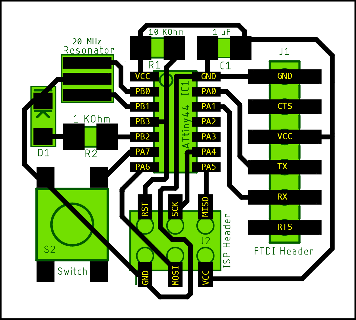
Finally, I came up with this schematic for the board;

Using the tools in eagle, I tried my best to produce an efficient board that could be milled and stuffed effectively.

I used the move and rotate tool to move the components around the space to create a layout that was best suited for the circuit board. I then used the wire tool to connect the components effectively and in an organised fashion. Once I was happy with layout of the circuit, I exported the files as a .dxf file that could be read by illustrator. The purpose of bringing the file into illustrator is to transform it into a .PNG image file that could be used by the milling machine to produce the board.

The final outcome of my board looked like this;

Unfortunately, there were too many students using the milling machine at this point, so I was unable to mill and stuff the end result. However, I am very pleased with the final result of the circuit board; I feel that my design is concise and should work as intended.


3D Scanning and Printing

This week’s task was to scan and prep an object to be 3D printed. To begin the session, Des spoke about the different methods of fabrication that work to print physical objects. We spoke about ABS, PLA and flexible printing in terms of materials. During this session, we also talked about the different software that could be used to edit and fix 3D scans (eg. Meshmixer or Meshlab). For the ease of use, I chose to use Meshmixer as it was free to download and seemed to be the easiest to pick up.

We then went over to the 3D printing suite to further understand the process of 3D printing. At the 3D printing suite, Des gave us a demo of the 3D scanning process using the university scanners. we were told to be slow and to maintain a consistent distance from the object that we would be scanning. This would allow the software to fully scan to the best of its ability.

We then finished the session by taking it in turns to 3D scan an object of our choice. For this, I chose to scan my camera (shown below).

The end result of my scan looked like this when loaded into meshmixer;


As a result of the scanning process, the scanner also picked up data from the table that the camera was sat on. In order to remove this, I used the select tool to select just the surface (seen in orange in the image below) and then used the ‘x’ shortcut on my keyboard to remove the surface.

Following this, I then used the ‘make solid’ tool to ensure that any gaps in the object were filled (seen below).

Unfortunately, I was unable to attend the class where we 3D printed the scans due to external complications. However, I would love to further understand the process in the future and finish a project involving 3D printing.

I am pleased with the scan I was able to make, however I feel that I could possibly do a better job if I had more time and multiple attempts to scan the object with more detail.

Lazer cutting intro

Using the Laser Cutter

Today we learnt about using the laser cutting machine. The machine allows us to ‘print’ shapes by cutting them out of certain materials on a flat, two axis system.

In order to print using the laser cutter, you must first prepare files for the cutter to receive. These files are often made using a CAD program such as Fusion 360. For the purposes of this task, I decided to use illustrator as it was available to me at the Edward Street campus and I am familiar with the Adobe suite.

We learn about the uses of laser cutting in digital fabrication and how it can be used to produce accurate cuts on various materials such as cardboard, card, paper, wood etc. In order for the laser cutter to work safely, we learnt about the use of the extractor that was linked to the cutter to draw out any smoke or fumes from the material as it was being cut. Obviously this is a risk to the operators health as fumes could cause all sorts of damage to the human. Adding to this, we were told to always use the machine whilst under the supervision of a member of staff and that we should never leave the machine as the risk of fire is always present.

Before cutting, it is important to set up the machine so it is zero’d and set to cut your chosen material. After placing your material in the top left corner (or wherever is required), the first step is to set the pointer to your prefered home point. This is done by pressing the pointer and then the X/Y off button on the panel. The laser head is then movable and the home point can be set. The home point is the origin; where the lazer will begin the cutting job. After these steps are done, the home can be set by pressing the ‘Set Home’ button on the front panel. The final step to calibrating the machine is to set the focus. Using the focus tool attachment, the user must press the up and down buttons on the panel in order to move the focus finder accordingly. The aim is to move the laser until the focus tool is just touching the material you plan to cut. This is done to ensure that the laser is in the prime location for cutting the materials as per the user’s settings.


Cutting

For this task, I decided to create some printing frames that I could use in the darkroom on my photography course. I needed the frames to be the same size as a 6×7 medium format negative, so I first measured the dimensions accurately in millimetres and then transferred them into illustrator.

The dimensions for the sketch were 620mmx750mm & 560mmx7mm. These two boxes allowed me to produce a frame accurate to my requirements.

I planned to cut these frames out of foam board as I felt this to be a suitable, cheap and light material to suit my needs. Before cutting the foam board, I did some research into whether or not there would be any issues regarding cutting this material. Upon researching, I found a forum post on Intructables.com (https://www.instructables.com/community/Safety-of-laser-cut-foamboard-fumes-etc/) in which users stated that foam board is usually created with Isopentane, Polystyrene and Talc. This would mean that when burned it would emit “styrene, carbon monoxide and other hydrocarbons”. This could be damaging to health in large amounts, however the ventilation should prevent a damaging amount of this gas to affect me or others. I checked with Andrew and he said that it would be fine to use this material.

With my sketch being made in illustrator, it was just a case of choosing File>Print and selecting the properties tab. This brought me to the settings tab for the Helix laser cutter that was linked to the computer. First, I checked that the piece size was correct. The setting should be 609mm (horizontal) x 457mm (vertical) to be calibrated to the bed size of the laser cutter. I then started to experiment with the speed and power of the laser; it became apparent very fast that if the laser was set to be too powerful, it would melt the foam board and affect the structure of the frames. Below, you can see the issues found with this in some tests I cut initially.

In order to work against this, I lowered the power of the laser and gradually decreased the speed to a point at which the material was able to be accurately cut without deforming the structure. I found that the optimal settings were 25% speed and 25% power.

Below shows the end product of the cutting process:

Below is a picture of the frames being used during darkroom work for my project:


Programming an ISP

This week, I worked on programming my stuffed board in order to complete it’s functional design. Using a USB connection for power and a ribbon connection for data transfer, I was able to successfully create a link between the computer and the board. Using the code provided by the FAB Academy, I was able to load the code onto the ISP Board.

Using the information from http://fab.cba.mit.edu/classes/863.16/doc/projects/ftsmin/index.html I was able to follow the instructions to sucessfully upload code onto my ISP and program it properly.

As I was using a Mac, I had to download CrossPack, a development environment specifically made for AVR microcontrollers.

Following this, I then downloaded the firmware source code that would be uploaded to the board. This was provided through a download link on the aforementioned blog post.

Once I had these two bits of software downloaded, I was able to upload the source code onto the board.

I first had to address the makefile to ensure that the code was adapted for my microcontroller. In order to do this, I found the line that says “PROGRAMMER ?= usbtiny” and found that no action was required as my code was already set for my microcontroller (see picture below).

Following this, I then opened the Terminal app and ran ‘make flash’ the idea of this is to remove the information form the target chip in order to replace it with the code we want uploading to the ISP. This didn’t quite run succesfully the first time as I had mistakenly inserted the ribbon connector in upside down. Once I had noticed this, I inverted it and retried the ‘make flash’ command. This successfully uploaded the code to the flash. At this point, I configured the fuses; the idea of this is to allow the ISP to program other boards without the board itself to be re-programmed.

To run this command, I typed ‘make fuses’. After a brief loading screen, the command went through as successful.

Finally, I needed to blow the reset fuse to ensure that no other code can be uploaded to the microprocessor. After checking that the usb was recognised by the Mac (Apple, About This Mac, More Info) I then ran the process ‘make rstdisbl’ The aim of this was to reset the fuses and ensure that no other code could be uploaded in the future.

Once the loading screen successfully ended, I removed the solder bridge from the board to ensure that the wire had been broken, creating a physical barrier to stop any code being loaded into the microprocessor.

Below is a short video showing the code process history. Unfortunately, I had not made photographs as I went along on this occasion.

IMG_4382

Electronics production

In this week, we learned about the production of circuit boards. Specifically, we’ve been learning about designing and milling our own boards with a view to producing one at the end of the task.

For the task this week we were asked to stuff a FabTinyISP. An ISP is an ‘in-system programing’ unit that is used as a pathway to load new information onto a circuit board. The purpose of creating an ISP is to have our own hardware that would be able to program future circuit boards.

Prior to us stuffing the boards, Andrew gave us an introduction to the basics of current and orientation of the components. He explained that current runs “alphabetically”; Anode to cathode. This gave me enough context to confidently begin stuffing the ISP board.

To begin the process, Andrew gave us all a milled board, list of components and a circuit board diagram to follow. With this information, I began to stuff the board, using the diagram as a guide to follow.

Above is the list of components given to us by Andrew

Above is the circuit diagram and schematic.

Using the provided information I was able to successfully stuff the ISP board. As I made my way through the board, I made sure to solder the components from the inside to the outside of the board. This made the process much easier to navigate around in order to accurately place each small component. When stuffing the board, I was very careful to follow the diagram to the best of my ability. The only issue I had was when I accidentally soldered a 1K ohm resistor in the place of a 499 OHM resistor. In order to rectify this issue, I applied a small amount of heat to the area to loosen the solder and allow me to easily remove the component without damaging it. Once I had fixed this issue, I continued to stuff the board with no further problems.

Above is a gif that shows the process of soldering each component to the board (you may need to click on the image to load the gif file).

To finish off the task, I soldered the bridge on the board. This bridge gives a computer access to the board in order to program the ISP. The bridge is shown in the picture below:

I am pleased with the outcome of this exercise as I feel that I now have a much better understanding of the board stuffing process as well as the practical understanding of how a circuit board flows current through each component.

The next part of the process is to load on the code to the board in order for it to function as a FabTinyISP. Once this has been done, I will be able to remove the solder bridge to ensure that no other data can be loaded onto the board.

Soldering Practice

This week, we practiced soldering ahead of our future assignments which would require difficult soldering of components. The session began with Andrew discussing the context of the assignment and what we would be doing over the next three weeks in order to produce different electronics as part of this module.

The practice circuit board was a very simple circuit that consisted of 10 LED’s and 5 1K Ohm resistors.

On the board, you can see the ‘G’ and ‘V’ symbols on the left and right respectivley. These symbols stand for Ground and Voltage. Not only does this direct the user to where to attach a current to the circuit, but it can also tell the person who is soldering the direction of current.

When soldering a circuit, the current flows from voltage to ground. 

We use this logic to understand which orientation to solder the components in. For example, the LED’s have a small arrow on the underside which points in the direction of the current’s flow.

Following the guidence of Andrew, I soldered the 10 LEDs by using the ‘tacking’ technique; I first applied some heat to the board, the applied some solder until a small amount had melted. I then applied pressure to the LED to allow them to ‘stick’ to the solder that was already applied to the board. Once this first half of the component is soldered, it keeps the component stuck to the board and allows for easier soldering of the second half of the component.

I then continued this tacking technique, throughout the remaining components until the circuit was complete.

Designing a Tile using Fusion 360

I have attempted to make my own tile design using fusion 360.

for my design, I wanted to recreate a kind of parquet flooring style. As you will see, I have created something of that effect, however I haven’t been able to produce a design that tiles in the same fashion to that of parquet flooring.

I began by creating two rectangle shapes that would act as my repeating design.

Using the move tool, I then rotated these two rectangles so that I could begin my repeating design.

Following this, I then used the rectangular pattern tool to multiply the design. I needed to multiply the pattern enough times to fill the 100x100mm tile size requirement from the breif.

Once I had my repeating pattern, I then used the recangle tool to create the 100x100mm square shape to act as a template for where I needed my design to work within.

After setting these parameters, I then used the trim tool to remove any sections of the design that went over those boundaries.

at this point, I was left with my tile design that was constrained to the dimentions mentioned in the breif. In order to start giving this design more texture, I chose to excrude the design and layer the different sections at different heights.

At this point, I was happy with the different levels I had created, I decided to add some colour to the design by using the appearance tool. I then considered my design to be finished.

I am pleased with the design of my tile, however I feel that I could do some mathmatical work into making the final product repeat in a fluent pattern. I also need to do work to understand how to retain the entire design once it has been excruded. You can see that some of the elements have combined once I excruded the design.